Knowles – The Capabilities, Benefits, and Key Applications for StackiCap
Power electronics demand higher capacitance in smaller packages, from industrial to automotive to aerospace applications. Therefore, electronic designers cannot continue adding more capacitors to meet both capacitance demands and size requirements. While capacitor stacking is an option, many stacked assemblies are still quite large, and stacking often introduces new failure modes, such as piezoelectric cracking (Figure 1).

To overcome this issue, many capacitor manufacturers’ solutions use special, stronger dielectric formulations, but these usually come with trade-offs regarding dielectric constant, and therefore the ultimate capacitance value available.
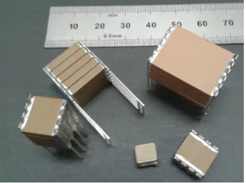
Figure 1. Various stacked assemblies up to an 8060 five stack.
Knowles Precision Devices offers a solution designed to provide high capacitance value (CV) in a compact package while reducing the risk of piezo electric cracking. Known as StackiCap™, this surface-mount multi-layer ceramic capacitor (MLCC) offers the greatest volumetric efficiency and CV per unit mass of any high-voltage X7R ceramic capacitor available. Figure 2 shows how single StackiCap components can replace various stacked assemblies. The electrical details of StackiCap are shown in Table 1.
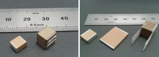
Figure 2. The image on the left shows a 2220 500V 1μF StackiCap that can replace a 2225 3 Stack 500V 1μF while the image on the right shows a 3640 500V 3.3μF StackiCap against 8060 and 3640 5 stack alternatives.
| Electrical Details | |
| Voltage Range | 200V – 2,000V |
| Maximum Capacitance | 5.6µF |
| Temperature Coefficient of Capacitance (TCC) | ±15% from -55°C to ± 125°C |
| Dissipation Factor | ≤ 0.025 |
| Insulation Resistance (IR) | 100GΩ or 500secs (whichever is the less) |
| Dielectric Withstand Voltage (DWV) | Voltage applied for ± 1 seconds, 50mA charging current maximum |
| Ageing Rate | < 2% per decade |
The Technology Behind StackiCap
With a novel and patented* inbuilt stress relieving layer, StackiCap capacitors exhibit the electrical and physical behavior of multiple, thinner components while exploiting the manufacture and process benefits of being a single unit. The stress-relieving layer included in StackiCap is made of a combination of already utilized material systems and is formed during the standard manufacturing process. The layer is positioned in the place(s) where mechanical stress is the greatest, which allows for the mechanical decoupling of the multiple component layers.
To further reduce the risk of mechanical stress damage, StackiCap terminations use our proprietary FlexiCap™ flexible termination material. Coupled with the fact that there is no need to attach components to form a stack, StackiCap does not require lead frames, which means we can use standard tape and reel packaging with pick-and-place capability for StackiCap.
Key Applications that Can Benefit from Using StackiCap
Between our unique patented construction and FlexiCap™ termination material, our StackiCap™ range of MLCCs are suitable for a variety of applications, including power supply filtering, lighting, aerospace electronics, DC-DC converters for industrial and automotive markets, and other high voltage applications where a large amount of capacitance is required. The majority of our StackiCap MLCCs are also AEC-Q200 qualified.
Overall, our StackiCap range of MLCCs significantly reduces required PCB real estate for an equivalent capacitance value when board space is at a premium.